WESTAK CIRCUITS
  • Company
    • About Westak
    • Locations
    • Careers / Benefits
    • Industry Certifications
    • Corp Responsibility
  • Engineering
    • Support
    • Design Guidelines
    • Materials
    • Stack Up Considerations
    • Tooling Package
    • IPC-D-356A Netlist
  • Capabilities
    • Westak Facilities
    • Global Alliances
  • Support
    • Request For Quote
    • Data Transfer Options
    • Contact Us
    • Supplier Requirements

Tooling Package

Creating Complete Tooling Packages

​Below is an overview of the package requirements for providing a detailed quotation, DFM report or complete manufacturing build. While we strive for flexibility with our customers, by providing the necessary information in a clear and organized format, we are able to maintain and expedite lead-times as well as increase the quality of manufactured product.

Company Specifications

A copy of your company’s approved workmanship standard or specification should accompany the first quote request and/or order placed. Additionally, suppliers should receive subsequent revisions to ensure they understand your current standards.
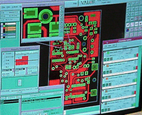
Design Data

​Electronic data from a PCB CAD system is generally required for manufacturing printed circuit boards. If all you have is artwork, we can assist you in translating that into electronic files. 
Picture
Picture
Picture
Data Elements to Include:
  • Inner and Outer layers (all copper layers)
  • Soldermask layers
  • Legend (silkscreen) layers
  • Aperture list (if not embedded with gerber RS274X or ODB++)
  • Image file supplied for each phototool, with clear description of the function of each file.
  • File function described both within the image data and in explanatory documentation.
  • 1:1 profile in one of the preferred formats is recommended
  • Solid copper areas designed as a “contour” or surface area, versus “painted”. (This can be achieved in many CAD systems utilizing correct output parameters and RS274X.)
  • Pads “flashed” with standard aperture shapes, rather than “painted” with lines
  • Verify Power/Ground files do not extend excessively beyond board edge (min .025”)
  • Use separate Dcode / aperture for multiple impedance circuitry on the same layer
  • Avoid cross hatching for thieving / copper distribution
  • Avoid output coordinate format of lower resolution than the CAD design database. This can cause registration issues and irregular edges on drawn “painted” features.
Solder Mask Elements to Include:
  • Design component holes and Test point locations as pad master (same diameter as O/L pads)
  • Designate plug or cap locations for tented or partially covered pads
Preferred Formats:
  • Valor ODB++
  • Gerber RS274X (embedded aperture format)
Picture

Drill Files

Netlist File

The drill files should include the following information:
  • Tool codes and X-Y coordinates
  • Each hole/slot size (finished diameter), with tolerance
  • Quantities for each hole/slot size
  • Hole/slot status (plated or non-plated), (via, press-fit)
  • Drill data alignment with design data
  • Separate drill files for blind / buried vias
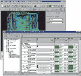
A CAD net list should be extracted from the design data and provided with the file transfer. The net list is used to verify the integrity of the design and to generate the associated test programs.

Preferred Format:
  • IPC-D-356A

Fabrication Notes / Drawing

Detailed notes should be provided to explain how the PCB should be manufactured. The drawing must clearly describe the part profile using standard dimensions and tolerance practices.
  • Board outline dimensions; including cutouts, chamfers, radii, bevels, scoring, etc.
  • Dimension from at least one drilled reference “non-plated” hole internal to the part
  • Hole chart with symbols, finished hole sizes, tolerances and quantity
  • Identify blind or buried vias
  • Material requirements (avoid specific product names, unless necessary for design)
  • Layer stack up
  • Finished board thickness and tolerance
  • Controlled impedance requirements (if applicable)
  • Surface finish specification
  • Notes defining product specifications to be used in fabrication
  • Notes defining any special requirements
  • Explicit solder mask, via cap, via plug or via fill instructions
Picture
Fabrication notes and the drawing are critical to a successful build!

Panelization Guideline

Picture
Contract Manufacturers generally have a preferred method of panelizing boards into an array. We need the following information to meet those requirements:
  • Existing array configuration with dimensions (if applicable)
  • Maximum panel array size
  • Preference for v-score or tab route breakaways
  • Rail size and location
  • Fiducial locations

ReadMe File

To ensure effective communication, we ask that a README file be included with files. The following information is recommended:
  • Contact name(s), email address and phone number (specify 24-hour contact if different)
  • Part number and revision
  • Complete listing of files, prints and net list
  • File format descriptions
  • Information on merging of files (if applicable)
  • Intentional short / open information (actual nets)

Company

About Westak
​Locations
Careers/Benefits
Certifications
Corp Responsibility

Engineering

Support
Design Guidelines
​Stack Up / Impedance
Tooling Package
​
IPC-D-356A Net List

Capabilities

Westak Facilities
Global Alliances

Support

Request For Quote
​Data Transfer Options
Contact Us
​Supplier Requirements
Picture
Picture
Picture
Picture
Picture
© COPYRIGHT 2023. ALL RIGHTS RESERVED.
  • Company
    • About Westak
    • Locations
    • Careers / Benefits
    • Industry Certifications
    • Corp Responsibility
  • Engineering
    • Support
    • Design Guidelines
    • Materials
    • Stack Up Considerations
    • Tooling Package
    • IPC-D-356A Netlist
  • Capabilities
    • Westak Facilities
    • Global Alliances
  • Support
    • Request For Quote
    • Data Transfer Options
    • Contact Us
    • Supplier Requirements